FAQ
If you have a question, please send them our way using the form to the right or ask directly in one of our support forums.
1. Availability
1.1. Where can I buy Alorium Technology products?
Alorium’s boards and modules are currently available
1.2. Will Alorium sell the bare FPGA for users who want to build their own board around it?
Yes, that is a model that we are open to discussing. However, we do not keep an inventory of pre-programmed FPGAs in stock, so we would need to handle it on a case-by-case basis.
2. General
2.1. What is the difference between "XLR8 Technology" and an "XLR8 Board"
It is a bit confusing in that XLR8 refers both to the underlying technology implemented on the FPGAs of each of our board types, as well as to our first board, the XLR8 Board.
The XLR8 Board is our first board, designed to be a drop-in replacement for the Arduino Uno board. It is compatible with the Uno while also be extendable through the XLR8 Technology.
Our XLR8 Technology includes the AVR compatible core embedded into the FPGA as well as the software support we’ve added to the Arduino IDE to enable the ability to load new FPGA images directly through the IDE. This has been extended even further in our OpenXLR8 Methodology that enables the ability to create completely custom hardware modules that are tightly integrated with the AVR core while maintaining the ability to load those custom OpenXLR8 images through the Arduino IDE.
2.2. Is there special software required to program an XLR8/Snō/Hinj?
No. XLR, Snō, and Hinj are all programmable with the Arduino IDE for programs/sketches and uploading new FPGA images supplied by Alorium Technology.
If you want to create custom Xcelerator Blocks for the FPGA, Intel’s Quartus Prime Lite FPGA design tool is required. More information on that process can be found here: OpenXLR8 Methodology.
2.3. How do you tell XLR8/Snō/Hinj to use its floating point hardware instead of using lots of clunky Arduino instructions?
In order to access their floating point hardware, we provide a library that you include in your sketch, but there are some changes required to the floating point arithmetic operations in your sketch, as well. Our library defines functions that directly access the general purpose registers within the processor core, such that the hardware-based floating point operations can be performed extremely fast. Any floating point operation that you want to accelerate in your sketch (or in any libraries you’re using) needs to be converted into the XLR8-specific function call. For example:
c = a + b;
becomes
c = xlr8FloatAdd(a,b);
Because I’m a lazy typist, I typically do this:
#define xA xlr8FloatAdd
so the line of code I end up with looks like:
c = xA(a,b);
There are similar functions for subtract, multiply, and divide, too. We debated a few different approaches for this, and landed on this one for the time being.
2.4. Does AloriumTech have plans to develop a dual core or hyperthreaded version of the board?
2.5. Is it possible to use a toolchain other than the Arduino IDE with XLR8?
C/C++ programs can be directly compiled with avr-gcc, makefiles, etc., and uploaded using avrdude over the USB/UART interface. It’s not a path that we use every day, but we do it occasionally. It’s a great way to avoid some of the overhead of Arduino’s built in libraries. Programming the chip via the ICSP header instead of through USB/UART is not supported. The Arduino optiboot bootloader is currently hardcoded into the design. It’s a pretty good bootloader, taking just 256 locations (512bytes) from the instruction memory. The ATmega’s “fuses” don’t really exist in our design, and the options they control are set to the Arduino defaults.
2.6. Will XLR8/Snō/Hinj include support for non-AVR cores in the future?
The Arduino ecosystem supports a number of different processor architectures. Because the AVR core seems to be the most prevalent core, and specifically because of its limitations, we wanted to offer an upgrade path to help Arduino users with a large base of AVR code to dramatically improve performance.
Down the road, user demand will help us decide on additional upgrades for our hardware solutions.
3. Arduino Compatibility
3.1. What chip is used for the USB to serial interface?
For XLR8 and Hinj, we use an FT230XQ FTDI chip.
The Snō board does not have a USB connector and requires an FTDI breakout board such as the SparkFun Beefy 3 Basic FTDI Breakout.
3.2. Is the microcontroller cycle accurate with a standard ATmega microcontroller?
3.3. Is it possible to run the CPU faster than the standard ATmega runs?
Yes, it can be. We provide FPGA images at both the standard 16MHz clock rate and a 32MHz clock rate. Switching to the faster clock rate does not affect the timers as we adjust them for the faster clock.
3.4. Does the implementation of the AVR core have the same memory available as the standard ATmega328 part?
XLR8, Snō and Hinj all provide the same program/flash and data/
However, there is extra memory on the FPGA that can be used in an Xcelerator Block. For instance, we have
In addition, the Hinj board provides the ability to double the program memory (PMEM) size to 64KB by uploading the latest image to the Hinj board through the Arduino IDE.
3.5. Does XLR8 have the same analog I/O capabilities as the Arduino Uno?
XLR8 has built-in ADC functionality just like the Arduino Uno, but a few of the specifics are different. We don’t have the option for an internal bandgap reference, nor do we have the ATmega’s analog compare function.
On the plus side, XLR8 will give correct ADC results regardless of whether it’s powered from USB or from the barrel connector, unlike an Arduino board which, when powered from USB, will give incorrect ADC readings due to a reduced 5v supply.
Additionally, the MAX 10 ADC is higher performing in both speed (1MHz) and resolution (12 bit) than the ATmega ADC, so look for future enhancements to XLR8 that will make these additional capabilities readily available to users!
3.6. Is SPI supported on the same pins as on the Uno and the ICSP pins?
3.9 SPI
The SPI interface on XLR8 should operate the same as the SPI interface on an Uno or Redboard. The only item to note is that we’ve seen some SPI examples where the XLR8/Uno/Redboard is the SPI slave and instead of being driven from the SPI master, the SS pin is left floating. XLR8, due to its I/O pullups, needs to have SS driven and not floating.
4. FPGA
4.1. What FPGA is used on the XLR8, Snō and Hinj boards?
XLR8, Snō and Hinj all use the Intel MAX 10. XLR8 uses an M08 sized MAX 10, Snō uses an M16, and the Hinj uses an M50.
5. OpenXLR8
5.1. Can I create my own Xcelerator Blocks for XLR8?
Yes. The OpenXLR8 methodology allows users to create completely custom logic blocks using a free toolset. These custom XBs are tightly integrated to the AVR core on the FPGA so that they are accessible via normal AVR in/out instructions.
You can learn more about OpenXLR8 here: OpenXLR8 Methodology
5.2. How much space is available on the FPGA for XBs?
The microcontroller uses about 80% of the available space on the 10M08 MAX 10, which is used on the XLR8 board.
If your custom OpenXLR8 logic doesn’t fit on the XLR8 board, try using the Snō board instead as it has an M16 MAX 10 which provides much more area for custom logic.
5.3. Can I burn my own FPGA image to XLR8/Snō/Hinj?
5.4. Is it possible to use the board I/O from the OpenXLR8 XBs?
It is certainly possible to use the board I/O from the OpenXLR8 XBs. We’ve tried to document how that is done both in the OpenXLR8 Webinar and in the openxlr8.v verilog file itself, in the form of comments. You can find the discussion of I/O at the 11:14 mark of OpenXLR8 Webinar, part 3: http://bit.ly/2t25O14
In addition, you can find additional examples by looking at the openxlr8.v file in some of the prebuilt XBs such as XLR8SPI. If you look at the openxlr8.v for the XLR8SPI (http://bit.ly/2sZWwCL), you can see inputs being used at lines 195-198, and outputs being assign at lines 282-307.
.
6. XLR8 Board
6.1. What is XLR8's digital I/O's voltage capabilities for input and output?
The long answer is, well, longer. The FPGA on the board has I/O that support 3.3V for inputs and outputs. On the digital pin input side, we have a FET-based circuit that limits the voltage seen by the chip to about 3.3V, so the inputs would correctly be categorized as 5V-tolerant. On the digital pin output side, again the chip is a 3.3V device, so it only drives to 3.3V. We have a 1K-ohm pull-up resistor on the board that pulls the signals up to 5V at the board interface, so what you’ll see at the board level is true 0-5V signalling.
The analog pins are a bit different. Those can also be configured as digital I/O on an Arduino, and the same is true on XLR8. There is a slightly more complex circuit to manage the inputs, since we want to be able to have the 3.3V ADC on the chip work over a 0-5V analog voltage range. The net is that, when used as digital inputs, those pins are also 5V-tolerant. However, we don’t have the pull-up resistors on those pins, so when configured as digital outputs, they will drive from 0 to 3.3V, and not to 5V.
7. Sno Board
7.1. Does the Sno Board have additional I/O over the XLR8 Board??
Yes, it has 18 additional GPIO pins.
7.2. Why can't Quartus see the Sno JTAG connection?
The USB blaster drives its outputs very hard which results in signal reflections due to impedance mismatches. With respect TCK in particular, there is both a large overshoot followed by an undershoot. The undershoot is significant enough in magnitude to cross the switching threshold and results in double clocking.
The external symptom is usually that no JTAG chain is detected. SnōMākr consistently masks the issue through altered impedance characteristics. When configuring Snō alone, we recommend a stiff pulldown (less than 250 ohms) on TCK, as close to the Snō board as possible. We have seen cases where a pulldown as low as 150 ohms is required.
There are other ways to address this, such as a custom harness with a series drive resistor (40 ohms or so), as close to the blaster as possible. The previous method, however, should work, and certainly will confirm that TCK undershoot is the issue.
8. Hinj Board
8.1. What interfaces come standard on the Hinj PMOD connectors??
There is a SPI, I2C and UART interface on PMOD-a, PMOD-B, and PMOD-C, respectively
8.2. Why is the built-in USB Blaster listed as "unconfigured"?
If you connect both mini-USB ports to a computer at the same time, then they conflict with each other. This causes some confusion on the PC so that it will indicate the USB Blaster as “unconfigured” and will not recognize the USB Blaster in Quartus Programmer. Only one of the mini-USB connectors should be used at a time.
8.3. Why does the FPGA upload process quit for my Hinj board?
If you are using the Arduino IDE to upload a new FPGA image to your Hinj board as described in Section 5 of the Hinj Quick Start Guide, AND you are using a Mac, the FPGA upload process may seem to terminate before the programming is complete.
For example, instead of seeing the expected completion message:
INFO: Arduino: Using port /dev/cu.usbserial-DB00KO28
Switching FPGA configuration to existing image 1
INFO: Complete
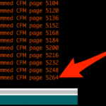
The output in the log will simply stop after programming the last CFM page:
This problem appears to be a communication issue between the Python code that coordinates the FPGA image upload and the Arduino IDE when running on a Mac.
Even though the process appears to fail, it has successfully completed the programming. The FPGA has been uploaded with the new image, but for some reason, the last bit of output does not make it to the console log.
NOTE: You must do a power cycle on your Hinj board in order for it to load the new image.
We have not yet been able to determine why this is an issue for the Mac version of Arduino IDE but not for Windows nor Linux. In addition, this issue does not occur when updating XLR8 or Snō boards.
8.4. I'm having trouble using the default PMOD interfaces
Please update your Hinj board to the latest FPGA image using the Arduino IDE. If you still have issues after upgrading then please send an email to support@aloriumtech.com
9. SnōMākr Board
9.1. What is the best method and components to mate the Snō connections to the SnōMākr connections?
The cleanest way (but probably the most challenging) is to solder the Snō board directly to the SnōMākr with no headers at all. If you line up the Snō to the SnōMākr, it’s possible to flow solder through the vias of both boards simultaneously and create a direct connection between the boards. As I mentioned, this is a bit challenging to do, and it also would make it very difficult to separate the boards if you wanted to in the future.
Another approach that is still very clean and compact is to use pin headers as the interface between the boards. We often use something like this:
https://www.sparkfun.com/
You’ll need a couple of those, since there are 59 connections between the boards. Soldering is much easier, and you still end up with a very clean solution. Future disassembly will also be challenging with this solution.
Finally, you could use headers on the SnōMākr board, and pins on the Snō to create a plug-in solution. We’ve used these:
https://www.sparkfun.com/
https://www.sparkfun.com/
This creates a very clean, low-profile solution that allows shields to still be used with the SnōMākr, and allows the Snō board to be removed if needed.
As far as a sequence, it comes down to accessibility of the pins with the soldering iron. You’ll want to use a small tip on the iron, and in general start with pins toward the center of the board and work your way out. If you’re soldering the boards together with no headers (again, the most challenging option listed above!), you’ll want to be very careful to avoid melting the SnōMākr headers as you’re reaching between them to solder.